Take a look at the highest-resolution image of atoms ever seen. Cornell University researchers captured a three-dimensional sample from a crystal and magnified it 100 million times, doubling the resolution that earned the same scientists a Guinness World Record in 2018. Their research could aid in the development of materials for more powerful and efficient phones, computers, and other electronic devices, as well as longer-lasting batteries.
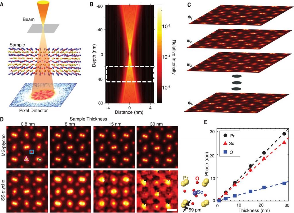
The image was created using a technique known as electron ptychography. It involves directing a billion-plus electron beam at a target material. As the electrons are fired, the beam moves infinitesimally, causing them to hit the sample from slightly different angles each time—sometimes they pass through cleanly, and other times they collide with atoms and bounce around inside the sample on their way out. The technique is similar to playing dodgeball against opponents who are standing in the dark, according to Cornell physicist David Muller, whose team conducted the recent study. Electrons are the dodgeballs, and individual atoms are the targets.

Muller can’t see the targets, but thanks to advanced detectors, he can see where the “dodgeballs” end up. Based on the speckle pattern generated by billions of electrons, machine-learning algorithms can calculate where the atoms were in the sample and what their shapes might be.
Electron ptychography had previously only been used to image extremely flat samples, such as those that were only a few atoms thick. It can now capture multiple layers tens to hundreds of atoms thick, according to a new study published in Science. As a result, materials scientists who study the properties of samples with a thickness of 30 to 50 nanometers will find the technique much more useful. (That range is smaller than the length your fingernails grow in a minute but many times thicker than what electron ptychography could image in the past.)
“They can actually look at stacks of atoms now, so it’s amazing,” says Andrew Maiden, an engineer at the University of Sheffield in England, who helped develop ptychography but was not involved with the new study. “The resolution is just staggering.”
Such high-resolution imaging techniques are essential for developing the next generation of electronic devices. For example, researchers are looking for more efficient semiconductors to replace silicon-based computer chips. Engineers will need to know what they’re working with on an atomic level to accomplish this, which will probably require the use of technologies like electron ptychography.
“We have these tools sitting there, waiting to help us optimize what will become the next generation of devices,” says J. Murray Gibson, dean of the Florida A&M University–Florida State University College of Engineering, who was not involved in the new study. “Without these tools, we couldn’t do it.”
Batteries are a particularly promising area for applying imaging techniques such as electron ptychography, says Roger Falcone, a physicist at the University of California, Berkeley, who was also not involved with the research. “How do we make the structure of batteries,” he asks, “such that they can store a lot of energy and yet still be safe?” This is an essential question, especially for the transition from fossil fuels to renewable energies, including wind and solar. “Imaging technologies are very important to improving batteries because we can look at the chemical reactions in detail,” Falcone says.
However, there is still much to be done. Electron ptychography must be capable of precisely locating an individual atom in a material in order to lead to a new breakthrough for your cell phone or laptop. The researchers have not yet performed an experimental demonstration, despite demonstrating how the technique could theoretically do so. Though the researchers demonstrated how the technique could do so theoretically, they have not yet performed an experimental demonstration. “With any new technique, it always takes a bit of time for your fellow researchers to try this out and see if it bears out into real, practical uses,” says Leslie Thompson, former manager of materials analysis and characterization at IBM Research–Almaden, who was not involved in the new study.
READ MORE: The Earth Has a Pulse: 27.5-Million-Year Cycle of Geological Activity Discovered